
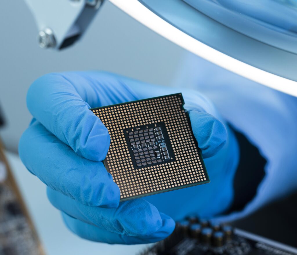
“Overcoming the Challenges in Wafer Fabrication: Innovative Solutions”
“The Multi-Step Process of Wafer Fabrication for Semiconductor Production” “Wafer Fabrication: Key to Producing High-Quality Semiconductors for the Electronics Industry” Despite the advancements in technology, wafer fabrication continues to face challenges that affect the yield and quality of the end product. The challenges in wafer fabrication and the solutions that have been developed and how […]
“The Multi-Step Process of Wafer Fabrication for Semiconductor Production”
“Wafer Fabrication: Key to Producing High-Quality Semiconductors for the Electronics Industry”
Despite the advancements in technology, wafer fabrication continues to face challenges that affect the yield and quality of the end product. The challenges in wafer fabrication and the solutions that have been developed and how to overcome.
Lithography Process Challenge:
The lithography process is the most critical stage in wafer fabrication. The process involves creating patterns on the wafer surface that will later be used to create the electrical circuits.
The challenge in this process is to produce patterns with high accuracy and resolution, which is becoming increasingly difficult with the shrinking of feature sizes.
This has led to the development of Extreme Ultraviolet (EUV) lithography, which is a more advanced technology that provides higher resolution and accuracy.
Deposition Process Challenge:
Deposition is the process of adding material to the wafer surface. The challenge in this process is to deposit the material evenly, without creating any defects.
This is particularly challenging for materials that have low melting points, such as copper, which can easily form voids.
To overcome this challenge, various techniques have been developed, including physical vapor deposition (PVD) and chemical vapor deposition (CVD).
Etching Process Challenge:
Etching is the process of removing material from the wafer surface to form the desired patterns. The challenge in this process is to control the etching rate and selectivity, which is crucial in achieving the desired pattern.
To overcome this challenge, various techniques have been developed, including dry etching and wet etching.
Doping Process Challenge: Doping is the process of introducing impurities into the wafer to create a desired electrical property. The challenge in this process is to control the concentration and distribution of the impurities, which is crucial in achieving the desired electrical properties.
To overcome this challenge, various techniques have been developed, including ion implantation and diffusion.
Quality Control Challenge: Quality control is a critical aspect of wafer fabrication, as it ensures that the end product meets the desired specifications.
The challenge in this process is to detect defects at an early stage, as they can become more difficult to detect as the process progresses.
To overcome this challenge, various inspection and testing techniques have been developed, including electron microscopy, X-ray diffraction, and optical microscopy.
Cost Challenge: Wafer fabrication is a costly process, and the cost continues to increase as the feature sizes shrink.
The challenge is to reduce the cost while maintaining the quality of the end product. To overcome this challenge, various cost-saving measures have been developed, including automation, process optimization, and the use of more cost-effective equipment.
Despite the complexities involved, the semiconductor industry has managed to overcome the challenges in wafer fabrication through the implementation of cutting-edge technologies and methods.
The introduction of EUV lithography, refined deposition, etching, doping techniques, and advanced quality control measures have enabled the production of top-notch semiconductor chips with reduced feature sizes and cost-effectiveness.
As technology continues to evolve, it is anticipated that these challenges will be addressed, promising a promising outlook for the electronics sector.